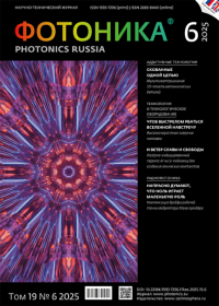
Issue #6/2025
M. S. Kovalev, N. G. Stsepuro, E. V. Ulturgasheva, S. I. Kudryashov
Single-pulse Laser-Induced Al Transfer Onto the Si Wafer for Ohmic Contact Development
Single-pulse Laser-Induced Al Transfer Onto the Si Wafer for Ohmic Contact Development
DOI: 10.22184/1993-7296.FRos.2025.19.6.466.477
Bauman Moscow State Technical University (National Research University), Moscow, Russia
The article examines the aluminum contacts on silicon wafers developed by the laser-induced forward transfer. It is determined that a single-pulse regime with an energy density of 15 J/cm2 leads to an aluminum concentration of 18.6% and a minimum contact resistance of 439 ± 4 Ohm. The method simplifies the contact generation process and eliminates the need for complex cleaning, making it promising for future silicon-based electronic applications.
Tags: direct laser writing laser-induced forward transfer (lift) ohmic contacts optoelectronics silicon кремний лазерно-индуцированный прямой перенос (пипп) омические контакты оптоэлектроника прямая лазерная запись
Subscribe to the journal Photonics Russia to read the full article.
Readers feedback

 rus
rus


